

| Using a base-collector strapped transistor as AM detector, sharper knee for better weak signal demodulation |
The emitter on such an NPN transistor would be the cathode, and the base tied to the collector is the anode Here I used a 2SC2785 salvaged from a VCR or such. If the transistor is a PNP, its emitter would be the anode, and its base tied to its collector the cathode. Try various transistors. I found that 680K seems to hit the sweet spot in this radio, but it's not a critical adjustment on a trimpot (which you can use to quickly find the value you'd want in a fixed resistor). I had thought that using a transistor this way was the mark of a sloppy company (did they run out of diodes?), but I got the best weak station detection performance with this. Oh, check strong stations too, which worked well too.
Turns out I needed a bit more sensitivity in the AVC detector diode, so I used a germanium
transistor with its base and collector strapped together. I found that physically larger transistors
have lower base-emitter drops (the 2N1304 has 0.14V with the base and collector tied together) than smaller germanium transistors. But be aware that most larger germanium
transistors may not be up to switching fast enough to act as a detector. I used the 2N1304,
its data sheet says it can do a few MHz. I now get less or no distortion on very strong stations,
as the AVC now kicks in with less "delay" ("AVC delay" means the AVC needs a certain voltage
amplitude before the AVC starts reducing the stage gain); it's not time delay.
 The big transistor with heat shrink over it is the large germanium
transistor. Its case is tied to its collector, and the heat shrink is to prevent shorts.
The big transistor with heat shrink over it is the large germanium
transistor. Its case is tied to its collector, and the heat shrink is to prevent shorts.
One another copy of this radio, I found that I really don't need a separate AVC diode. The AVC circuit produces enough bias on the new transistor-as-diode to get good demodulation on weak stations. Measure the diode drop voltage with a DVM with this feature, and find a transistor-as-diode with a similar drop to replace the diode with.
On yet another version of this radio, it turned out I needed a separate AVC detector, now "D3". The audio detecting
transistor (this set used silicon) strapped as a diode "Dau" needed less bias current than the AVC circuit imposed on this diode.
If the AVC circuit imposed less of the current the "diode" needs
for its sweet spot for best audio detection, one could add a resistor to B+ to get the current on the
diode into that sweet spot (the immediately above radio had this AVC current already on the sweet spot).
But it's not so easy to reduce the AVC current, so I added a
2nd diode "D3" to provide the AVC action. Oh, you need bias current on the audio detector
diode "Dau", else you may not hear anything. 390K to +5V put the new diode in its sweet spot.
The weak AM reception is now better, and this set lives up to its badge as a "Musaphonic" radio.


Some simulations of a silicon diode, a base-collector strapped silicon transistor,

![]()
and such a transistor with a bias current.
![]()
I'm not sure how much, if any, knee can be below 0V here. Conduction on the other side of 0V would probably mess up the
detection. IIRC, the FCC requires that 10% be the minimium amplitude of an AM station's carrier,
which should permit some knee curvature of stations that aren't too weak (else signal to noise
would make them unlistenable anyway).
Source web page. "AM detector more sensitive than simple diode". EDN September 28, 2016
by Lyle Williams
I modified this circuit a little, mostly changing the diode to a diode strapped transistor,
for a sharper detection knee. I also kept the old detector in place in my radio to take
care of AVC (but moved the volume control to the output of this new circuit (and used a
resistor to substitute for the volume control resistance in the AVC circuit)).
Below left my modified schematic. Q1 is essentially a current amplifier, turning on at the peaks of the AM modulated signal, to charge up C2 and R2 (filter, time constant circuit). This briefly turns Q1 on at the AM signal peaks, charging the filter cap C2. And R2 bleeds this charge off between times. Q1 also keeps a high impedance load on the detector, like an emitter follower at the AM peaks. I found that putting C2 right at Q1 avoids regenerative heterodyne whistles, as it keeps the RF circulating currents in a small area, reducing coupling into the AM antenna. The RC filter time constant essentially includes the B+ supply bypass cap to get to ground. This detector operates on the positive peaks, while the AVC circuit operates on the negative peaks.
The AM signal is a 455KHz carrier with 1kHz modulation at 100%. The input impedance of the detector
is around 300kO, which doesn’t appreciably load the source. The transistor Q2 strapped as a diode is operated with
a slight forward bias so a regular silicon transistor can be used. The output
impedance of the circuit is low and the load here has little effect on the distortion level.
Here the usual AVC circuit in the AM section of this radio gets an assist from a JFET
operating as a voltage controlled resistor. This is in the triode or ohmic region (at and near
0V and 0mA current, the blue region in the figure below) where the FET can operate as a
voltage-controlled resistor. The triode or ohmic region in an FET is sometimes known as the linear region. The
JFET operating as a voltage-controlled resistor works in this region.
If we extend the VDS voltage range to include slightly negative voltages for a particular
gate-t-source voltage, we see that the there is still a resistive effect. Preferably, there
is no DC voltage across the JFET’s drain and source terminals in the voltage controlled resistance mode.
This JFET's source and drain is connected across the
entire LC circuit of the first IF transformer, which has no significant DC across it.
The source and the drain both have IF frequency energy on them, out of phase with each other.
The LC circuit has a tap near the center of the winding, tied to
an RF ground (which is why the drain and source has out of phase IF energy)
The gate is roughly at the midpoint of the resistance, which should reduce the effect of
the gate capacitance on the IF. When the gate voltage VGS here is dropped below around
-4V, the JFET (a J211) becomes near infinite resistance. At around -2.7V, the JFET becomes a resistance around
1500 ohms. This variable resistance across the IF transformer LC circuit attenuates the signal strength,
and also as a side benefit, will make that LC circuit have wider bandwidth. Which will allow
higher audio frequencies from the strong station to be heard, higher fidelity (also better
fidelity because the attenuation keeps the strong station from overdriving and distorting in the rest of
the IF strip). Weaker stations will have narrower passbands, avoiding "monkey chatter"
from immediately adjacent weak stations. The controlling
voltage is acquired from the AVC line via an inverting transistor (a 2N2222). This transistor level shifts
and amplifies the AVC voltage range. Weak signals create a higher AVC voltage, and the transistor
goes into more conductance, drawing, via the collector resistor, its collector voltage more negative. Strong signals will
produce lower AVC voltages, and the transistor goes nearly into cutoff, and the collector approaches
the positive supply rail.
Be sure to use a bypass cap between this collector and the B+ line, to avoid ripple and such
from "modulating" the voltage controlled resistances of the JFETs. Which would distort the detected audio.
You need to size this cap to smooth out ripple, but still allow the circuit to respond to
the AVC changing due to tuning in stations.
I used a trimpot to get a sweet spot of an emitter resistor value, setting the gain of this transistor
(a value that has the JFET do nothing on weak stations, but attenuates strong stations to minimize
distortion), then
I used a fixed resistor of this value in the finished circuit. Not a great way to do circuit
design, as variations in the transistors and JFETs could throw this off in production.
The IF transformer's LC circuit is also at the positive supply rail.
From the JFET's point of view, (its gate is connected to the transistor collector) its gate
going more negative makes the JFET resistance go higher. The gate getting less negative makes it
lower resistance, attenuating the strong station's signal. As the AVC circuit is a feedback loop,
the JFET's resistance will settle to a value after this loop does its action.
A second JFET
on the IF transformer between the first and second IF stages is also installed. You don't want to
put it at the last IF transformer, as all you'd do is attenuate distorted signal. A third JFET
is also used on the antenna LC circuit (I removed a 1.5pF cap there, as the JFET has some
internal capacitance, a few pF's, inside it). Then I retweaked the antenna trimmer cap.
Another radio, this one AM:
If you are okay with infecting a valve radio with solid state parts, then:
This radio is the classic All American 5ive hot chassis radio. This will work for transformer
powered sets too.
I wanted to avoid loading the AVC circuit itself. This above circuit shows what the AVC has
already done to the signal. Loading the AVC circuit directly would tend to make the AVC
circuit less effective in controlling the IF gain.
The FM section of the radio I put this in doesn't really have AVC, as you want the FM signal to get clipped
before the discriminator detector anyway. I can see a station with full
quieting still be intermediate signal strength, and stronger stations are of
course full quieting. This above circuit shows the varying levels of station
strength beyond full quieting (useful for antenna aiming). I tapped the 2nd to last
IF stage (TR7's collector in the schematic in the JFET section of this
page), where clipping hasn't fully kicked in yet, but full clipping does happen in the final
IF stage.
You know the old loose bipolar NPN or PNP transistor test method of checking the PN junctions (with
your DVM in diode mode), like
from the base to the emitter, and then base to collector. You can figure out if it's an NPN or a PNP
transistor (compare to a diode). And additionally, you can see some transistor activity by doing this
following test: First, having
one test lead on the emitter and the other on the base (but not the collector), in the direction you see a diode drop voltage,
typically you'd see about 0.68V on a silicon transistor. Now while keeping the same test lead on the emitter,
touch at the same time with the other lead both the base and the collector. You should see a lower
voltage like 0.59V (around 85% of just the base-emitter only value). This test can also tell you, with surface mount devices, if you
really have a transistor, or a device with two diodes, one with a common anode, or a common cathode on what would
look like the base pin.
![]()

The simulation input and output patterns are shown above right . The output audio waveform is shown
with the correct DC level with respect to the center line which is 0 volts. Note that the output
voltage does not go to zero even with 100% modulation. There is no visible distortion
in the output and that is unusual with 100% modulation.
Using a JFET as a voltage controlled resistor for variable IF bandwidth, and to act
like an AVC circuit in a transistor AM radio.
This circuit widens the bandwidth on strong stations
(adjacent stations are so weak you wont hear them), for more audio high frequencies, better fidelity.
Weak stations will have narrower passbands, avoiding "monkey chatter" from
immediately adjacent weak stations. I live 6 miles north of a 50,000 watt flamethrouer, WABC 770KHz.
They briefly played music to celebrate their past. This mod helped make it sound good, almost hifi.


Above right shows an exaggerated relation of passbands (how wide some value of X dB down) to radio station signal strngths. The
passbands really vary by a factor of two at most. Attenuation is related to AVC action, in
that weak stations are amplified more than strong stations in regular AVC circuits, and here
there is actual attenuation being done as well (which via the voltage controlled resistive JFETs
changes the passband widths of the various
IF transformers and the antenna LC circuit).

Here is a single JFET connected across the 2nd IF transformer T2. The IF amp transistor TR2 also
acts like the 2N2222 in the above AM/FM radios (as TR2's base gets biased by the
AVC line), and the JFET control signal is picked off a
bypassed resistor R10, was 1K, now 1.5K (to increase the control voltage range). The full LC
circuit of T2 is bypassed by C18 and biased by voltage divider R6 and R7. There was a diode
between T2 and R10, but I removed it before I added the JFET. The voltage divider was reworked
(by changing R6 to 180 ohms) to have the JFET go almost into infinite resistance when the radio is tuned to an empty
spot on the dial. And to drop resistance value on strong signals. This then widens the IF bandwidth
and reduces the IF strip's
gain.
Another AM radio, an RCA RZA202B, with the JFET mod. One JFET across the antenna LC circuit L1, and another JFET
across the first IF LC circuit T1. Driven by a similar buffer transistor that uses the AVC line voltage
and converts to to the JFETs' gate control.
The above mods on solid state transistor radios, using JFETs as variable
resistors across IF transformers. Idea
is to use the AVC voltage to increase or decrease the JFET resistance to assist the AVC function,
and to make received audio bandwidth on strong local stations wider. And perceived audio signal
levels are more even while tuning across the AM band. Someone asked about doing this on tube sets.
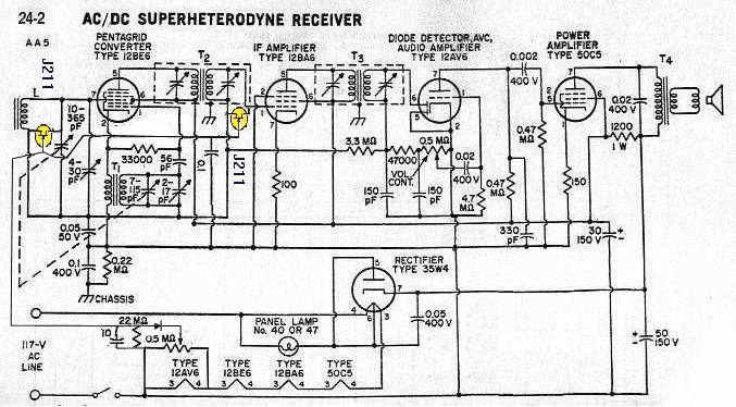
I put the JFET on the secondary of the 1st transformer. This secondary is riding on the AVC
voltage line. For the JFET I used (J211), to have infinite resistance, its gate should be around
-4V compared to its source and drain. About -2.7V gets about 1.5K resistance. Here, the source
and drain (connected to the IF transformer secondary) are riding the AVC voltage, and I'd need a
fixed negative voltage to connect the gate to. I used a half megohm trimpot on 12VAC (tapped the
heater string) then rectified that and filtered it to get an adjustable negative bias for the gate.
RF Bypass this bias to ground. I and added another JFET to the antenna circuit. JFETs add about
2pF of capacitance so you'll have to tweak the trimmers.
Simple radio receiver signal strength indicator, not using the AVC line
This circuit samples the voltage of the IF signal on a collector of a transistor in the IF amp.
And is independent of the AVC circuit. The diode D2 "detects" the amplitude of the IF signal
(the diode pointed so that more IF amplitude makes the bias on Q1 increase, thus making the LED
light brighter),
either 455KHz or 10.7MHz in an AM/FM set I put this into. Resistors R2 and R3 were a
single 470K trimpot I used to adjust the bias on Q1 (the wiper connects to the base)
to get the LED on Q1's collector to light or dim as I tune across the AM or
the FM dial. Measured the trimpot, and then used 39K for R3 and 560K for R2.
Your mileage will vary, depending on the diode you use for IF level detector D2 and transistor for Q1.
R1's resistance was chosen to be a negligible load on the signal
getting amplified by the IF stages of the radio. That then drives the selection of R2 and R3's resistance.
The LED is a modern high efficiency one that doesn't require much current to light up bright.
It came from a recently made Xmas light string. Thus Q1 doesn't need much biasing from the "detector"
circuit to delver enough current to light the LED.
How to test a bipolar regular or SMD transistor with a DVM in diode mode, to tell it
apart from a dual common anode or cathode diodes inside a 3 legged SMD devide.
![]()
![]()
![]()